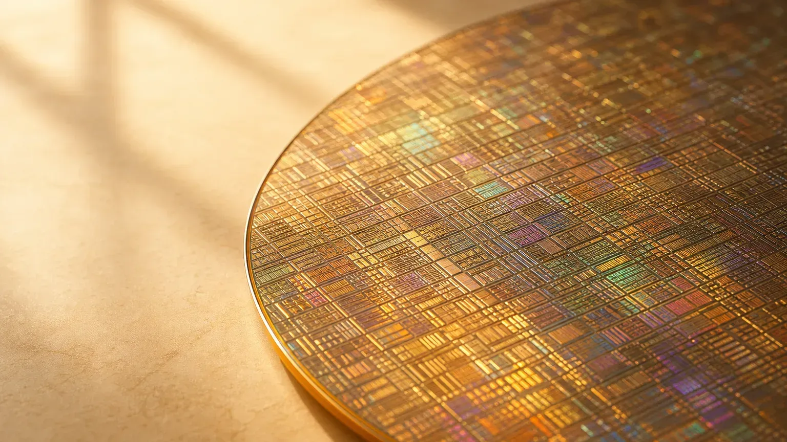
This is the TSMC 2nm deep dive for the foundry gate in The AI Hardware Supply Chain, End to End: what N2 is, who uses it, and where rivals stand. For a beginner overview of 2nm, 3nm, and GAA, see the advanced-process gate.
What N2 Is: TSMC’s First GAA Process
TSMC’s 2nm is called N2. It is TSMC’s first volume-production node to use nanosheet/GAA (gate-all-around) transistors, replacing the FinFET of the 3nm generation.
The difference is how the gate wraps the channel. FinFET is like a sluice gate walled on three sides; GAA adds the fourth wall. That gives better control of current and less leakage, so performance holds as transistors shrink. TSMC says the enhanced N2P, versus N3E, is about 18% faster at the same power, or uses about 36% less power at the same speed, with about 1.2x logic density.
Timeline and Fabs: Mass Production in 2025, Home Turf in Taiwan
TSMC says N2 entered mass production in Q4 2025, and it already made up 3% of TSMC’s wafer revenue in Q2 2026. Production is centered on Fab 20 in Baoshan, Hsinchu, and Fab 22 in Kaohsiung.
| Node | Key point | Timing |
|---|---|---|
| N2P | Enhanced N2 | Official: volume production in the second half of 2026 |
| A16 | Adds backside power delivery (Super Power Rail) | Media report (August 2026): development and verification complete, mass production in Q4; TSMC has not announced the start of mass production |
| A14 | The node after that | Official: risk production in 2027, mass production in 2028 |
Backside power delivery moves the power wiring to the back of the chip, freeing the front for signal wiring.
In Arizona, US, TSMC added US$100 billion in July 2026, bringing its total planned investment to US$265 billion. The new money goes to fabs at 2nm and below and to advanced packaging. The third fab is not expected to make N2 and A16 until near the end of this decade.
Who’s Using It: Phone Chips Ship First
TSMC doesn’t publish its customer list. The table below shows what customers have said themselves (as of October 2026):
| Customer | Product | How it’s confirmed |
|---|---|---|
| MediaTek | Dimensity 9600 Pro phone chip (announced 2026/9/15) | MediaTek says 2nm; Reuters reports TSMC 2nm |
| Qualcomm | Snapdragon 8 Elite Gen 6 / Extreme Gen 6 (announced September 2026) | A Qualcomm spokesperson confirmed TSMC 2nm to TechRadar |
| Apple | A20 Pro in iPhone 18 Pro (announced September 2026) | Apple says 2nm, without naming the foundry |
| AMD | Venice EPYC server processors | AMD official: on TSMC 2nm, production ramp from May 2026 |
Whether NVIDIA uses 2nm or A16 is, as of October 2026, still only market rumor. The newest nodes are expensive, so the first in line are usually chips that can pay a premium, like phone and server chips.
Pricing, Yield, and Capital Expenditure
TSMC doesn’t publish an N2 yield percentage or its wafer prices. Korean outlet ChosunBiz (September 2026), citing industry sources, said an N2 wafer costs about US$30,000 and 3nm about US$20,000. Treat that as a media report.
The official number is capital spending: in July 2026, TSMC raised its full-year capex guidance to US$60–64 billion, with 70–80% going to advanced processes.
Where the Rivals Stand: Samsung and Intel
Samsung’s first-generation 2nm (SF2) was already in mass production in 2025, and Samsung says it is ramping second-generation 2nm phone chips in the second half of 2026. Intel’s 18A (RibbonFET transistors plus PowerVia backside power) is in mass production across several products. The next node, 14A, is expected to start risk production in the second half of 2027 and mass production in 2028; as of October 2026, no customer has publicly committed to it.
Backside power is a common point of comparison: Intel 18A already uses PowerVia, while TSMC brings it in only with A16. Whose yields hold steady, and who gets customer products into volume smoothly first, will decide this race.
The Supply Chain and the Role of Taiwanese Firms
The most critical tool for N2 front-end manufacturing is ASML’s EUV. The pricier High-NA EUV is not required for 2nm: in September 2026, TSMC said it will bring High-NA into volume production at advanced nodes only from 2030.
For the “2nm theme stocks” often discussed in Taiwan’s market, analysts name firms in design services and silicon IP (such as GUC and Alchip), packaging and test (ASE and SPIL), substrates (Unimicron), photomask pods (such as Gudeng), and materials and equipment. These are possible supply-chain roles, mostly from broker and media guesses. Being named doesn’t mean a firm has N2 orders or shows how much it benefits. This article only describes industry roles and is not investment advice.
Penchan’s summary
N2 is TSMC’s step from FinFET to GAA, and in 2026 it is already inside flagship phone and server chips.
When you read 2nm news, first check who is saying it. Only what customers announce themselves counts as confirmed; yields, prices, and theme-stock lists are mostly media and analyst claims.
Further reading: foundry, EUV, the supply-chain overview.