
The news often says “TSMC starts 2nm volume production” or “Intel moves into GAA.” But is 2nm really 2 nanometers small? And what is GAA?
This piece explains the advanced process in plain words: what a process node really means, how the transistor evolved, where each company stands, and why more advanced means more expensive. It is the deep-dive version of the Foundry gate.
What Is a Process Node?
3nm and 2nm do not mean that some part inside the chip is really only 3 or 2 nanometers wide.
In the early days, the node number roughly matched the size of a transistor. Below 10nm, that link broke. Today it is the name of a “technology generation,” standing for a set of improvements: faster, more power-efficient, and denser transistors. That is why later generations got names like A16 and A14, counted in angstroms (0.1 nanometer).
How much does one generation improve? Take TSMC A14: its official target is 10-15% faster than 2nm at the same power, or 25-30% less power at the same speed.
Core-Data Snapshot
| Generation | Status | Source |
|---|---|---|
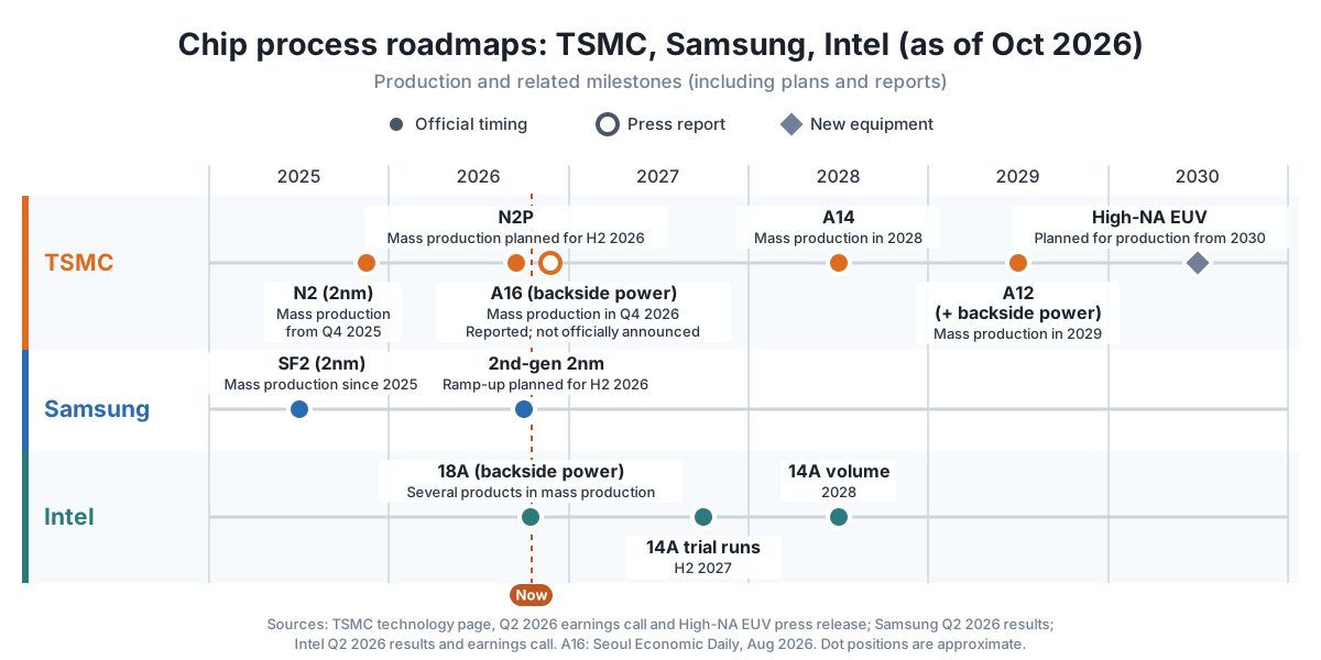
| TSMC N2 (2nm) | Volume production from Q4 2025; 3% of wafer revenue in Q2 2026 | TSMC official |
| TSMC N2P | Volume production planned for 2H 2026 | TSMC official |
| TSMC A16 (backside power) | Development and validation complete, volume production in Q4 2026; not yet officially announced by TSMC | Industry reports (August 2026) |
| TSMC A14 / A12 | A14 volume production in 2028; A12 (A14 plus backside power) in 2029 | TSMC official (July 2026) |
| Samsung 2nm (SF2) | Volume production since 2025; second generation planned to ramp in 2H 2026 | Samsung official |
| Intel 18A / 14A | 18A in volume production across several products; 14A risk production in 2H 2027, volume production in 2028 | Intel official (July 2026) |
How the Transistor Evolved: Planar → FinFET → GAA
Chips get stronger because transistors (tiny switches that turn current on and off) keep getting smaller. But the smaller they get, the more they leak, so the structure has had to evolve.
Planar transistor: the gate controls the current only from above. Once it shrinks, it loses control and leaks badly. FinFET: the channel stands up as a “fin,” and the gate wraps around three sides. It was used for several generations. GAA (gate-all-around): the channel becomes stacked horizontal nanosheets, and the gate wraps all four sides. It leaks less and fits more into the same area. Samsung used GAA first, at 3nm; TSMC starts with 2nm.
An analogy: planar is pressing on a water pipe from above with one hand, FinFET is cupping three sides with your palm, and GAA wraps all the way around.
2nm and GAA: Where It Stands Now
2nm is the generation where all three big makers switch to GAA. TSMC’s 2nm is in volume production, but in Q2 2026 it made up only 3% of wafer revenue. 3nm, at about 30%, is still the workhorse.
Since September 2026, 2nm has started to show up in flagship phones. Apple says the A20 Pro uses a 2nm process (Apple has not named the foundry). MediaTek’s Dimensity 9600 Pro uses TSMC 2nm. According to TechRadar, a Qualcomm spokesperson confirmed that the Snapdragon 8 Elite Gen 6 also uses TSMC 2nm.
Samsung and Intel are both in volume production, and Intel has even used High-NA EUV on some Panther Lake chips. Most performance numbers are targets; yield and customer adoption decide who wins.
Backside Power: The Next Move After 2nm
In a traditional chip, the power wires and signal wires are crowded together above the transistors, and the more advanced the chip, the worse the crowding. Backside power moves the power-delivery network to the back of the chip and leaves the front for signal wires. That cuts interference and improves performance and density.
Intel’s PowerVia is already in volume production with 18A. TSMC’s Super Power Rail is used in A16, and A12 in 2029 will use it too.
Why the Most Advanced Processes Are So Expensive and So Hard
Advanced processes eat three scarce resources at once.
First, equipment: they need ASML’s extreme ultraviolet (EUV) lithography machines, each costing hundreds of millions of dollars. The next generation, High-NA EUV (EUV with higher resolution), costs even more, and TSMC plans to use it in volume production only from 2030 (for details, see the ASML gate). Second, yield: a new structure takes a long time to bring the share of good chips up. Third, the design ecosystem: the more advanced the process, the more complex the design tools and rules.
These costs end up in the wafer price. According to a September 2026 report by Korean outlet ChosunBiz, a 2nm wafer costs about $30,000 and a 3nm wafer about $20,000.
Taiwan’s Role
Taiwan is the volume-production base for the most advanced logic processes. TSMC’s 2nm started volume production in Taiwan first, and in July 2026 TSMC said it will build 13 advanced-process and packaging fabs in Taiwan over the next few years. Its 2nm/A16 fab in Arizona, US, is planned to reach volume production before 2030.
This echoes the concentration described in the Foundry gate: a new process needs R&D, equipment, and talent working closely together, so the most advanced generation usually lands in Taiwan first.
Penchan’s summary
The key to the advanced-process race is mass production at a high enough yield.
Scaling keeps getting more expensive and harder, but it remains one of the fundamental sources of AI-chip performance. Whoever can reliably mass-produce the most advanced process holds the upstream of AI compute.
For the foundry landscape, go back to Foundry; for the equipment behind the process, see ASML; for how packaging takes the baton, see Advanced Packaging; for the whole chain, head back to the supply-chain overview.