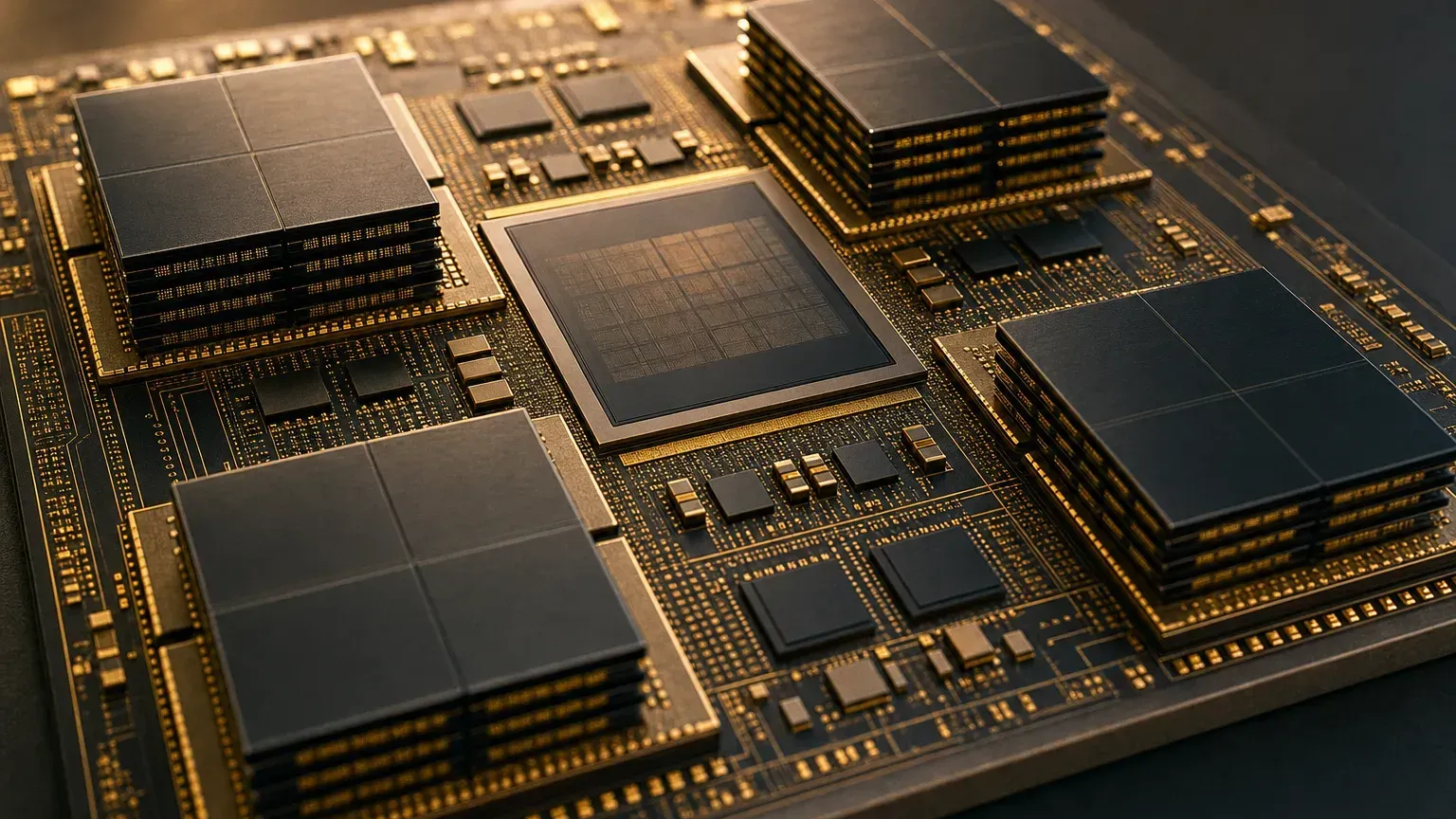
CoWoS is how TSMC binds a GPU and HBM into one giant module, but it is only one member of the “advanced packaging” family.
This piece extends Gate 3 of The AI Hardware Supply Chain, End to End. It covers what advanced packaging is, its main technology routes, and who does what in Taiwan’s supply chain.
What Is Advanced Packaging?
Traditional packaging is the back-end step after a chip is made: wrap one chip, connect its pins, and protect it. Advanced packaging combines several chips, such as one compute chip plus several HBM memory stacks, into one tight module. It uses a silicon interposer (a slice of silicon with ultra-fine wiring that acts as a bridge between chips), redistribution layers, or vertical stacking. The closer the chips and the shorter the wires, the higher the bandwidth.
An analogy: traditional packaging is like putting a jacket on a book. Advanced packaging is like stacking a few books and your notes in order and binding them into one handy reference volume.
Why AI Needs Advanced Packaging
Chips used to get stronger mainly by shrinking transistors. But at 3nm and 2nm, each further step costs much more and gets much harder, so the industry now looks for performance in “how you put chips together.” High-end AI chips also have to pack a compute core and several HBM stacks into one package, which is impossible without advanced packaging. That makes packaging capacity one of the bottlenecks for shipping AI chips. On TSMC’s July 2026 earnings call, Chairman C.C. Wei said packaging capacity was so tight it was “limiting our customers’ growth.”
Core-Data Snapshot
TSMC does not publish its CoWoS capacity. The capacity figures below are analyst or media estimates, so read them for order of magnitude only.
| Item | Figure | Nature |
|---|---|---|
| TSMC 2026 capital expenditure | $60–64B, roughly 10–20% of it for advanced packaging, testing, photomasks, and similar | Official guidance (July 2026 earnings call) |
| CoWoS monthly capacity, end of 2025 | About 70k wafers | Media estimate |
| CoWoS monthly capacity, end of 2026 | About 130k–140k wafers | Analyst / media estimate |
| CoWoS monthly capacity, 2027 | About 200k–220k wafers | Analyst / media estimate |
| CoWoS monthly capacity, end of 2028 | About 260k wafers | Media estimate |
The Advanced-Packaging Family Tree: 2.5D, 3D, and Panel-Level
2.5D: chips side by side. The leading example is TSMC’s CoWoS: a compute chip and several HBM stacks sit side by side and connect through an interposer, like Lego bricks laid out on one baseplate. InFO replaces the interposer with redistribution layers and is common in phone chips.
3D: chips stacked on top of each other. The leading example is TSMC’s SoIC: it bonds chips vertically with contacts far thinner than a hair, like stacking Lego bricks upward. Distances get shorter and density higher, but yield is harder to keep up. TSMC’s official roadmap already runs to an A14-on-A14 SoIC in 2029. The two can be combined: stack a few small chips with SoIC first, then place them into a CoWoS module.
Panel-level (FOPLP): a square panel instead of a round wafer. A round wafer wastes its edges. A large square panel uses area better and suits bigger packages. ASE’s 310mm×310mm panel-level line targets volume production in Q1 2027 (according to TrendForce’s report on ASE’s July 2026 earnings call). TSMC’s version is called CoPoS. According to August 2026 media reports, its first line in Chiayi is complete and running, with pilot production expected in 2027 and volume production in the second half of 2028.
Taiwan’s Packaging-and-Test Supply Chain: Who Does What
TSMC: the most advanced CoWoS and SoIC. When capacity runs short, it brings in packaging partners. In June 2026 it signed a 10-year agreement with Amkor to buy advanced-packaging and test services from Amkor in Arizona, US (official announcement). Media also report that TSMC is outsourcing more of the front-end CoW step to ASE and others; TSMC has not confirmed this.
Contract packaging-and-test (OSAT): ASE Technology Holding, Amkor, Powertech. ASE Technology Holding (including its subsidiary SPIL) is the packaging-and-test leader, and its VIPack platform covers fan-out and 2.5D/3D. According to media reports, SPIL broke ground on a new CoWoS plant in Douliu, Yunlin, in August 2026, with Phase 1 set to operate in 2028. In September 2026 Amkor said it was expanding its Arizona campus investment plan to about $12B, and NVIDIA has also made prepayments to support Amkor’s US capacity. According to Commercial Times, Powertech’s advanced-packaging capacity in Taiwan for 2026–2027 is fully booked by AMD and other customers, and it has formed a joint venture with Broadcom in Singapore for panel-level packaging.
Testing: KYEC. Its core work is wafer probing and final testing to protect yield; it is not a main packaging assembler. Another firm, Chipbond, handles back-end steps for driver ICs, a different field from AI-chip packaging.
IC substrates: Unimicron, NanYa PCB, Kinsus. A substrate is the material that carries the chip and makes the electrical connections (high-end ones use ABF substrates). These firms sell materials; they don’t do contract packaging.
Equipment: Scientech, Grand Process Technology, Gallant Micro Machining (GMM), C SUN, and others. Their tools cover wet processing, temporary bonding, die sorting, and die bonding.
How to Read “Advanced-Packaging Concept Stocks”
The market often puts the whole chain above under “advanced-packaging concept stocks.” But these companies mostly keep their customers and orders confidential, so the pairings the market cites are often analyst guesses, and being named doesn’t mean a company has won orders. This article only describes industry roles. It does not list beneficiary stocks and is not investment advice.
Penchan’s summary
Further reading: What Is CoWoS, glass substrates, Taiwan’s semiconductor supply chain, or back to the supply-chain overview.
Advanced packaging has a simple role: shrinking transistors keeps getting more expensive, so precisely assembling several chips together has become another way for AI chips to get stronger. Read this page as a map of who is on the chain and what role they play. That is far more useful than treating it as a stock-picking list.