Advanced packaging is about how chips are put together, but the board that carries those chips has to keep up too. AI chips keep getting bigger and more power-hungry, today’s organic carrier boards are starting to struggle, and so the industry is turning to glass.
As of October 2026, the main players are still sampling, running reliability tests, and going through customer validation, and most mass-production targets sit in 2028 or later. This is the materials extension of The AI Hardware Supply Chain, End to End.
What is a glass substrate?
The carrier board (substrate) sits between the chip and the motherboard. It holds the chip and routes its wiring out. A common organic carrier uses a resin core, with insulating materials such as ABF and copper lines on the outer layers.
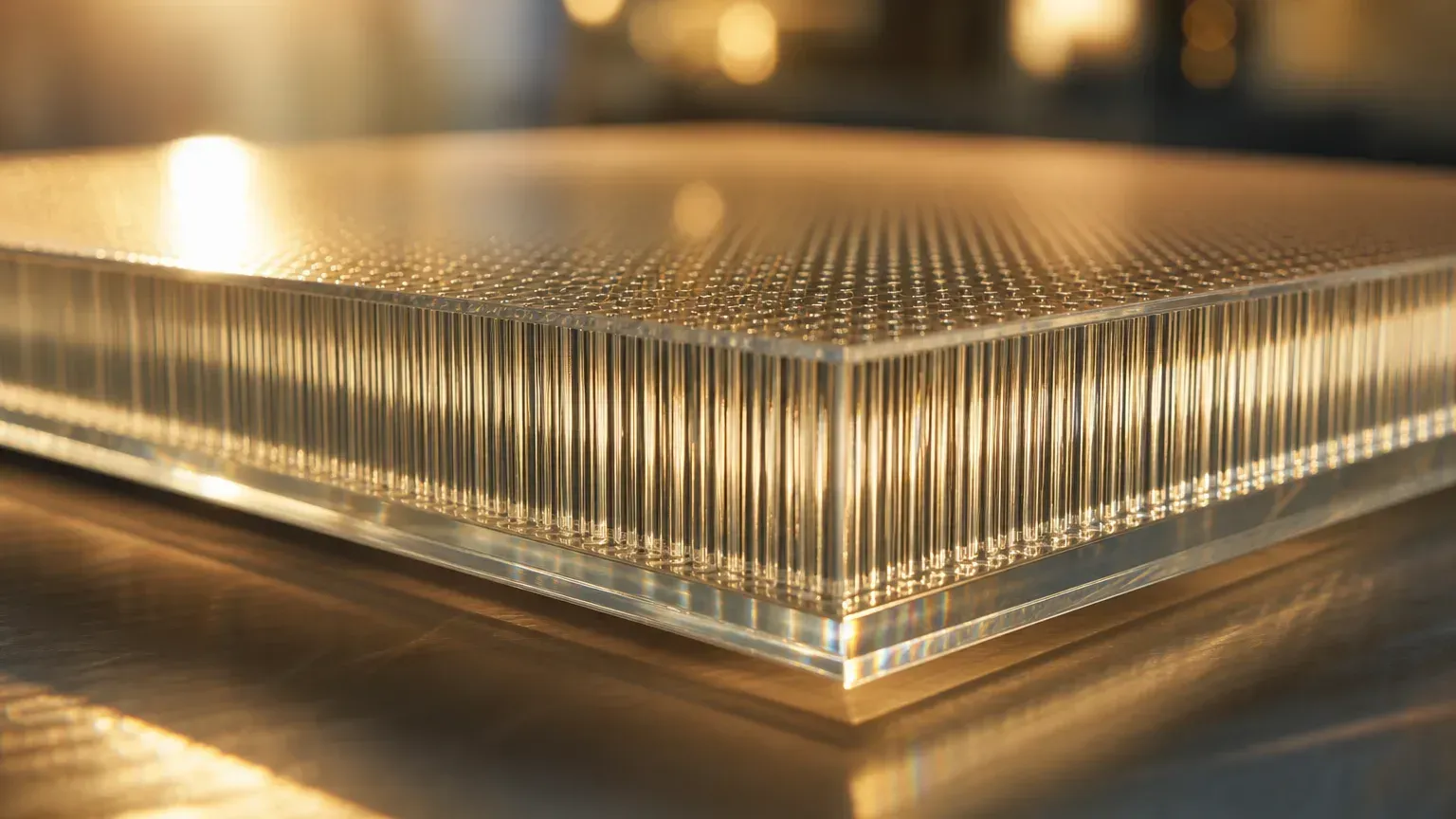
A glass substrate only swaps the carrier’s core layer for glass. The outer layers can still use ABF, so it is like replacing the innermost foundation. An organic core is like a wooden board that warps a little when heated; a glass core is like a flat, stiff pane of glass. The bigger the package, the more a stable foundation matters.
Advantages and challenges of glass substrates
There are three advantages:
- Flat and stable: it handles heat and resists warping, which suits large packages.
- Higher density: according to Intel’s white paper, through-glass via pitch is about 100 microns versus about 325 microns for organic carriers, for up to about 10 times the via density.
- Lower signal loss: good for high-speed data.
The challenge is that glass is brittle. Drilling and cutting can leave micro-cracks, and filling the vias with copper is hard. Both directly pull yield down.
TGV: the critical process for glass substrates
TGV (Through-Glass Via) means drilling extremely fine vertical holes in the glass, then filling them with copper or plating metal on the hole walls, so signals and power can pass between the upper and lower layers. Glass does not conduct electricity. Without these “elevators,” a glass core is just an insulating plate.
You have to drill fine, deep holes in hard, brittle glass without leaving cracks, and fill them evenly with copper. If TGV is not stable, a production line cannot reach mass production.
Progress of the international players
Public progress as of October 2026:
| Company | Progress | Mass-production timeline | Source |
|---|---|---|---|
| Intel | According to Tom’s Hardware, it has shifted to licensing patents and showing samples; it also plans a glass-substrate plant in India with 3DGS (about $3.3 billion) | Not announced officially; media estimate around 2030 | Media |
| Absolics (part of SKC) | Samples from its Georgia, US plant passed initial evaluation and are in reliability testing; the plant received up to $75 million in US CHIPS Act funding | Not announced by the company; media reports say either late 2026 or 2027 | Official (September 2026) |
| Samsung Electro-Mechanics | Evaluating customer samples on its Sejong pilot line | Glass core material in the second half of 2027; finished substrates in 2028 | Company statement (via media) |
| LG Innotek | 2028 (other reports say 2027–2028) | Media | |
| DNP (Dai Nippon Printing) | Started a pilot line in December 2025 | Fiscal year 2028 | Official / media |
Media often name AMD, Broadcom, AWS, and NVIDIA as potential customers, but according to Tom’s Hardware’s roundup, none of them has been officially confirmed.
Where Taiwan players stand in glass substrates
Working with glass and panel-level processes is a strength of panel makers, so the Taiwan player getting the most attention is Innolux. Its chip-first panel-level packaging is already shipping, but that is an existing application. TGV glass substrates for AI are still in customer validation, and its chairman said at the August 2026 earnings call that mass production would come in 2028 at the earliest.
Carrier-board maker Unimicron is more cautious. At its July 2026 earnings call, it said large-scale production before 2030 is unlikely, that glass substrates will be mainly custom products, and that they cannot replace existing carriers. AUO is also working on them but has not announced a mass-production timeline. According to Business Next, TPK has invested in a TGV pilot line, originally scheduled to start trial production in September 2026.
How to read “glass-substrate stocks”
The market often strings together panel makers and carrier-board makers, plus Scientech on the equipment side and Taiwan Glass and Fulltech Fiber Glass on the materials side, into a concept chain. Being on the list does not mean a company has orders, is in mass production, or is sure to benefit. It is more useful to read it as an industry map of who is staking out a position than as a stock-picking list. This article is not investment advice.
Mass-production timeline: when will it go mainstream?
SEMI (the global semiconductor industry association) thinks meaningful shipments are unlikely before 2028. TSMC is pushing its panel-level packaging, CoPoS, first, and media estimate its glass-core substrates will not be commercial until after 2030.
Penchan’s summary
Glass substrates are the next direction for packaging carriers, but they move forward on a scale of years. 2026 is a validation year, not a volume year.
What is worth tracking is which company first gets public customer certification and which line actually starts shipping, not which new name joins the concept-stock list.
Further reading: What is advanced packaging, CoWoS, Taiwan’s semiconductor supply chain, supply-chain overview.