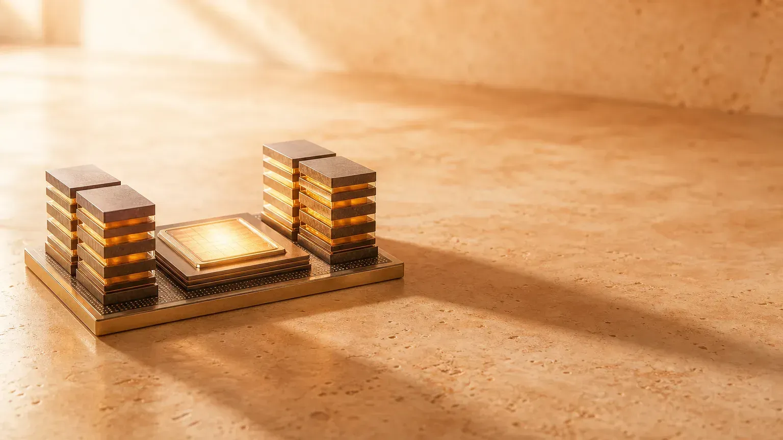
AI news often says “TSMC’s CoWoS capacity is sold out again.” But few people can explain what CoWoS is, or how one packaging technology can hold back shipments of AI chips.
This is the deep-dive version of Gate 3 in The AI Hardware Supply Chain, End to End, explained in plain words.
What Is CoWoS? One Sentence and One Analogy
CoWoS stands for Chip on Wafer on Substrate. It is TSMC’s 2.5D advanced-packaging technology. It places one GPU die and several HBM high-bandwidth memory stacks tightly together on the same “interposer,” then fixes that onto a substrate to form one large AI accelerator module.
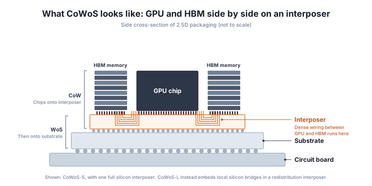
Here’s an analogy. Traditional packaging builds the chip and the memory separately, then connects them with wires on a circuit board. CoWoS is like gluing a few Lego pieces onto the same baseplate, so the two sit almost touching.
Why go to this trouble? Because the amount of data is huge. Take Nvidia’s Rubin: the bandwidth between each GPU and its HBM4 reaches 19.2 TB per second. Wires on a circuit board are too long, so the signal weakens and slows down. Remember it in one line: CoWoS lets a GPU and its memory work face-to-face.
How Advanced Packaging Relates to CoWoS
Advanced packaging is the broad category. It covers ways to place several chips very close together (2.5D) or stack them directly (3D). CoWoS is TSMC’s 2.5D version built for large AI chips.
CoWoS comes in three types. CoWoS-S uses one whole silicon interposer. CoWoS-R uses a redistribution-layer interposer made of polymer and copper lines. CoWoS-L embeds local silicon bridges in a redistribution-layer interposer, so it gets both a large area and dense connections.
Core-Data Snapshot
TSMC does not publish its monthly CoWoS capacity. Every figure below is an estimate from research firms or media, so just watch the growth slope.
| Time | TSMC CoWoS monthly capacity (wafers) | Source type |
|---|---|---|
| End of 2025 | About 70,000 | Media estimate |
| End of 2026 | About 130,000-140,000 (reports range 120,000-140,000) | Media estimate |
| 2027 | About 200,000-220,000 | Media and analyst estimates |
| End of 2028 | About 260,000 | Media estimate |
Why CoWoS Holds Back the Whole AI Supply Chain
Almost every high-end AI chip needs CoWoS or a similar package: Nvidia’s Blackwell, Rubin (which entered volume production in 2026), and Google’s TPU all do. Even when the wafers and the HBM are ready, a chip that can’t get a slot on the packaging line still can’t ship.
At TSMC’s July 2026 earnings call, Chairman C.C. Wei said packaging capacity is so tight it is “already limiting customers’ growth.” Research firm TrendForce estimates the shortage of this kind of packaging will only start to ease in 2027.
Who Can Make It? The Division of Labor Between TSMC and the Test Houses
The name CoWoS actually describes two steps: first the chips are attached to the interposer (CoW), then that is attached to the substrate (WoS). TSMC is by far the main player.
When demand is too full, TSMC hands some steps to assembly-and-test houses. In the past it mainly outsourced the back-end WoS step. In 2026, media reported that TSMC was also outsourcing more of the front-end CoW step to firms such as ASE; TSMC has not confirmed this. ASE’s SPIL unit broke ground on a new CoWoS plant in Douliu, Yunlin, in August 2026, and the first phase is expected to start operating in 2028.
Intel is also pushing its own EMIB-T packaging to compete. It says it will support customer volume production in 2027, but it has not named any customers. This division of labor is a starting point for understanding “advanced packaging stocks.” This article makes no investment judgment.
Why Taiwan Sits at the Center of This Chain
Most CoWoS capacity is in Taiwan. A high-end AI chip is first made with TSMC’s advanced process, then packaged with CoWoS, so the two tightest links sit on the same island.
The US build-out has only just started. In June 2026, TSMC signed a 10-year agreement with Amkor to buy Amkor’s advanced packaging and test services in Arizona. According to Reuters, a TSMC executive said the company plans to build CoWoS capability in Arizona by 2029. Until then, if supply from Taiwan were cut off, it would be hard to find the same amount of replacement capacity in the short term.
What to Watch Next: Bigger CoWoS, Glass Substrates, and Panel-Level Packaging
First, CoWoS keeps getting bigger. TSMC says CoWoS at 5.5 times the reticle size is already in production, and a 14-times version is expected to reach volume production in 2028. One package could then hold about 10 compute dies and 20 HBM stacks.
Second, the glass substrate, which replaces the traditional organic substrate with glass. Industry group SEMI expects little real volume before 2028, and Intel has not announced a volume-production date yet.
Third, panel-level packaging (TSMC calls it CoPoS), which moves packaging from round wafers onto square panels to make more units at once. Media report that TSMC’s first line was completed in Chiayi in August 2026, with trial production expected in 2027 and volume production around 2028.
None of these can replace CoWoS in the short term. They are more like the next generation waiting to take over.
Penchan’s summary
In this round of the AI race, “who can get CoWoS capacity” sometimes decides shipments earlier than “whose chip design is stronger.” Watching supply-chain bottlenecks often shows where things are heading sooner than watching product launches, and the core of this bottleneck is in Taiwan.
To read about memory that is just as tight, see What Is HBM. To see all eight gates of the chain, see The AI Hardware Supply Chain, End to End.