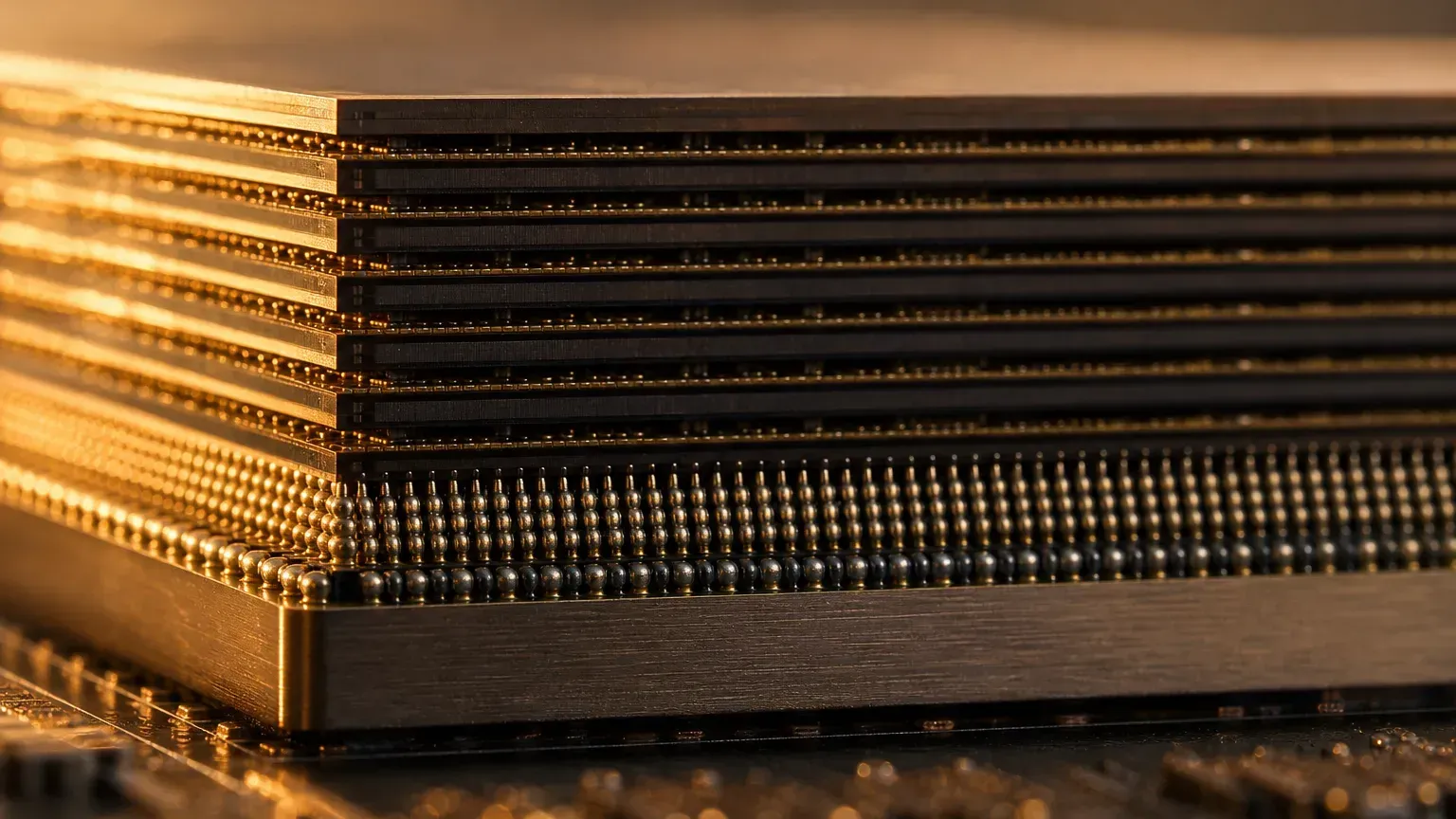
An AI chip can compute as fast as it likes, but if memory can’t deliver data in time, the compute cores just sit and wait. HBM4 is the new generation of high-bandwidth memory built to fix that. It’s what NVIDIA’s Vera Rubin uses, in volume shipments since August 2026.
If you’re new to HBM, start with the HBM gate.
What Is HBM4?
HBM (high-bandwidth memory) stacks several DRAM dies vertically and connects them to the GPU through a very wide interface. HBM3e is the version the Blackwell generation uses; HBM4 is the next one.
HBM4 changes the structure, not just the speed. Two things matter: the external interface doubles in width, and the base die at the bottom moves to a logic process.
Core-Data Snapshot
| Topic | Data | Nature |
|---|---|---|
| External interface | HBM3e 1024-bit → HBM4 2048-bit | JEDEC standard |
| Per-stack bandwidth | Standard ceiling about 2 TB/s; Samsung product up to 3.3 TB/s, Micron >2.8 TB/s | JEDEC standard / each maker’s product spec |
| Capacity | 4/8/12/16-layer stacks, up to 64GB per stack | JEDEC standard |
| base die | SK hynix uses TSMC 12nm-class; Samsung its own 4nm; Micron in-house | Media report (TrendForce, 2026-10) |
HBM3e to HBM4: What Changed
Interface width doubles: think of a highway widening from 1024 lanes to 2048 lanes. At the same speed, traffic nearly doubles. This is HBM4’s core upgrade.
Bandwidth jumps a level: mainstream HBM3e products run at about 1.2TB per second. HBM4’s standard alone reaches 2TB per second, and the makers’ products go beyond spec. When you see different numbers, first check whether it’s the “JEDEC standard ceiling” or “one maker’s product spec.”
Base die moves to a logic process: the base die at the bottom talks to the GPU. It used to be made on a DRAM process; from HBM4 on, it uses a foundry logic process, which can hold more control and custom features. That turns HBM from plain memory into a “memory plus logic” platform designed around each customer’s needs.
Better power efficiency: SK hynix and Samsung both claim HBM4 is about 40% more power-efficient than the prior generation. Micron claims over 20% for its own 12-layer product.
The Three Makers’ HBM4 Progress
HBM4 is still a three-way contest between SK hynix, Samsung, and Micron. All three reached mass production in 2026:
- Samsung: first to announce mass production and commercial shipments, in February 2026.
- Micron: its 36GB 12-layer HBM4 entered mass production in the first quarter of 2026, built specifically for NVIDIA’s Vera Rubin.
- SK hynix: first to announce completed development, in 2025; began volume shipments in the second quarter of 2026.
According to Korean media, Jensen Huang said in June 2026 that all three makers’ HBM4 had passed Vera Rubin qualification. The next contest is supply share and yield. Korea Herald cited industry estimates that about 60% to 70% of Rubin’s first HBM4 comes from SK hynix, about 25% to 30% from Samsung, and less from Micron. NVIDIA has not disclosed the split.
Taiwanese companies don’t make HBM itself. Their role is base die foundry work (TSMC) and the packaging and test around it; for who does what, see HBM stocks.
Next Step: HBM4E
HBM4E is an enhanced HBM4, and sampling began in 2026. Samsung says it shipped the industry’s first samples. SK hynix sampled a 12-layer, 48GB version in June and targets mass production in 2027. TrendForce expects HBM4E to ramp in the second half of 2027.
Customization goes further too. Micron says it is working with NVIDIA on the industry’s first custom HBM4E (NVHBM). According to TrendForce, Micron’s HBM4E base die will move to an outside foundry, and SK hynix’s will prioritize TSMC 3nm.
Why New AI Chips Need It
NVIDIA’s Vera Rubin carries 288GB of HBM4 per GPU, with 19.2TB per second of memory bandwidth. AMD’s MI455X also carries 432GB of HBM4. Inference-style, long-context AI moves far more data than before. Once memory falls behind, even the strongest compute cores just sit and wait.
In other words, HBM4 is the “conveyor-belt upgrade” for AI chips. Without it, no matter how much compute there is, memory becomes the bottleneck.
Penchan’s summary
For HBM4, remember two things: the doubled interface width buys bandwidth, and moving the base die to a logic process pushes HBM toward customization.
To see how packaging binds HBM and the GPU together, read CoWoS. To see all eight gates of the chain, head back to the supply-chain overview.
When reading HBM4 news, first check whether a number is the JEDEC standard or one maker’s product, and whether it’s sampling or mass production. Then the numbers won’t get mixed up.