When people talk about semiconductors, the spotlight usually lands on chip designers and makers like TSMC and NVIDIA. Go one layer further upstream and you find that the machines inside the fabs are built by a different set of companies. Without that equipment, even the best process is just a design on paper.
This piece first covers which machines it takes to make a chip and what each of the five global equipment makers does. Then it looks at where Taiwan’s equipment-and-materials firms stand. It is the wider-map companion to ASML and lithography equipment.
What Does Semiconductor Equipment Do?
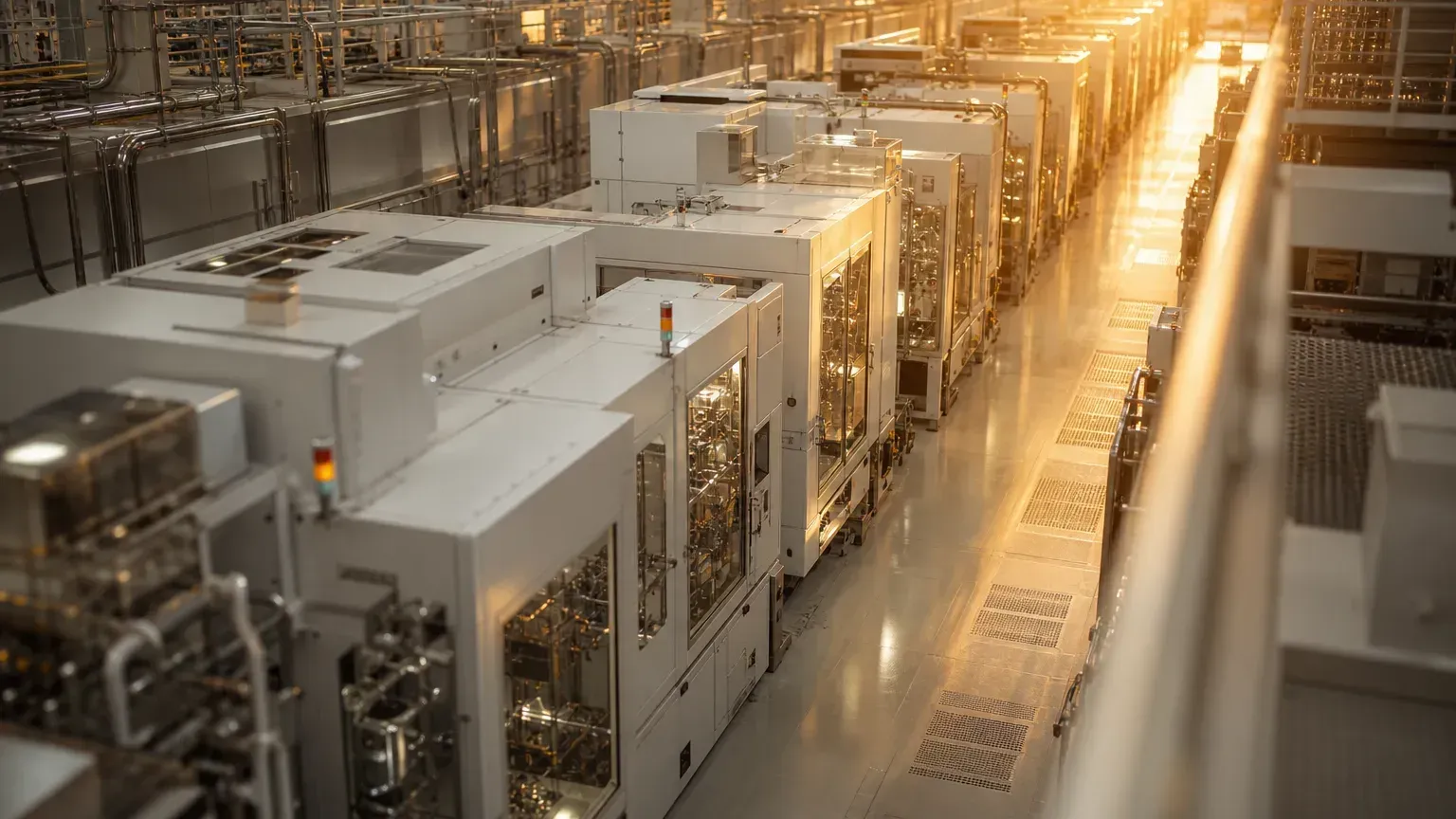
Making a chip means “building” tens of billions of tiny circuits on a silicon wafer. After a wafer enters the fab, it first grows a material layer and gets a coat of light-sensitive photoresist. A lithography tool “prints” the circuit pattern onto it. Then etch carves out the lines, and the wafer is cleaned and polished flat. Then the next layer is grown, printed, and etched again. This repeats hundreds of times, with defect checks all the way through. Each step has its own class of specialized machine. Together, they are “semiconductor equipment.”
Core-Data Snapshot
| Topic | Figure | Source |
|---|---|---|
| Global semiconductor-equipment market | $135.1B in 2025 (up 15% year over year) | SEMI actuals |
| 2026 forecast | $165.9B (up 23.2% year over year) | SEMI forecast, July 2026 |
| Top three markets (2025) | China $49.3B, Taiwan $31.5B, Korea $25.8B | SEMI actuals |
| Lithography leader ASML | €32.7B revenue in 2025, 48 EUV systems sold | ASML annual report |
| High-NA EUV (next-generation EUV) | First volume logic product in July 2026 (some chip layers of Intel 18A); TSMC plans volume adoption from 2030 | ASML, TSMC official |
The Main Equipment Categories and What Each Does
| Equipment category | What it does (in plain terms) |
|---|---|
| Lithography | Uses light to “print” the circuit pattern from the reticle onto the wafer’s photoresist; the most critical and most expensive step |
| Coat / develop (track) | Applies photoresist and develops it after exposure; works alongside lithography |
| Etch | ”Carves away” unwanted material along the pattern; comes in dry and wet types |
| Thin-film deposition | Grows thin films such as conductors and insulating layers (CVD / PVD / ALD) |
| Chemical-mechanical planarization (CMP) | Polishes the surface flat with a pad and slurry so the next layer can be stacked |
| Ion implantation | Shoots dopant ions into the silicon to change its electrical properties |
| Inspection and metrology | Measures linewidth, film thickness, and defects to protect yield throughout |
| Cleaning | Removes particles and residue; happens between many steps |
The World’s Five Big Equipment Makers
| Company | Main role |
|---|---|
| ASML (Netherlands) | The lithography leader and the only EUV supplier in the world |
| Applied Materials (US) | The broadest product line: deposition, etch, CMP, ion implantation, and metrology |
| Lam Research (US) | Etch, deposition, and cleaning; strongest in plasma etch at advanced nodes |
| Tokyo Electron (Japan) | Coat/develop, deposition, etch, and cleaning |
| KLA (US) | The leader in inspection, metrology, and process control |
Because the barrier is so high, equipment exports have become a geopolitical bargaining chip, and the US has tightened equipment exports to China several times in recent years. China is also a major customer for the big makers: in their quarterly reports from mid-2026, China made up 28% of revenue at Applied Materials, 26% at Lam Research, and 30.4% at Tokyo Electron. For the background on the rules, see export controls.
Taiwan’s Equipment Supply Chain: Who Does What
Taiwan is not a main producer of core tools like lithography or etch systems, but it has a full supply chain in many niches:
- GUDENG (家登): EUV reticle pods and wafer carriers, which keep reticles and wafers free of contamination.
- Scientech (辛耘) and Grand Process Technology (弘塑): wet-process equipment (cleaning, wet etch, and similar). Grand Process Technology also sells chemicals, and Scientech also does reclaimed wafers.
- Kinik (中砂): diamond discs and polishing consumables for CMP; a consumables role.
- Topco (崇越): materials distribution and integration, acting as agent for silicon wafers, photoresist, specialty gases, slurry, and more.
- Marketech (帆宣): fab facility automation and systems integration.
- MA-tek (閎康): materials analysis and failure analysis services; not an equipment or materials supplier.
- Gallant Precision Machining (均豪): automation and inspection equipment.
The market often groups these companies as “semiconductor-equipment concept stocks.” They are on a different scale from the global big five. Their actual customers, tool models, and orders are usually confidential, and the links the market draws are often institutional investors’ speculation. Being listed doesn’t mean a company already has orders or will benefit. This piece only describes industry roles. It doesn’t compile beneficiary stocks, doesn’t rank individual names, and is not investment advice.
Penchan’s summary
Semiconductor equipment is the very top of the supply chain, held by five global makers. Among them, ASML’s EUV is a gate that advanced processes can’t get around. Taiwan’s equipment-and-materials firms mostly work in niches such as carriers, wet processing, consumables, and materials distribution.
To see who this equipment serves, read foundry and advanced process. To see the whole chain, go back to the supply-chain overview.
Knowing the division of labor helps you judge quickly which link a news story touches. But a map of who does what is not a stock-picking list.